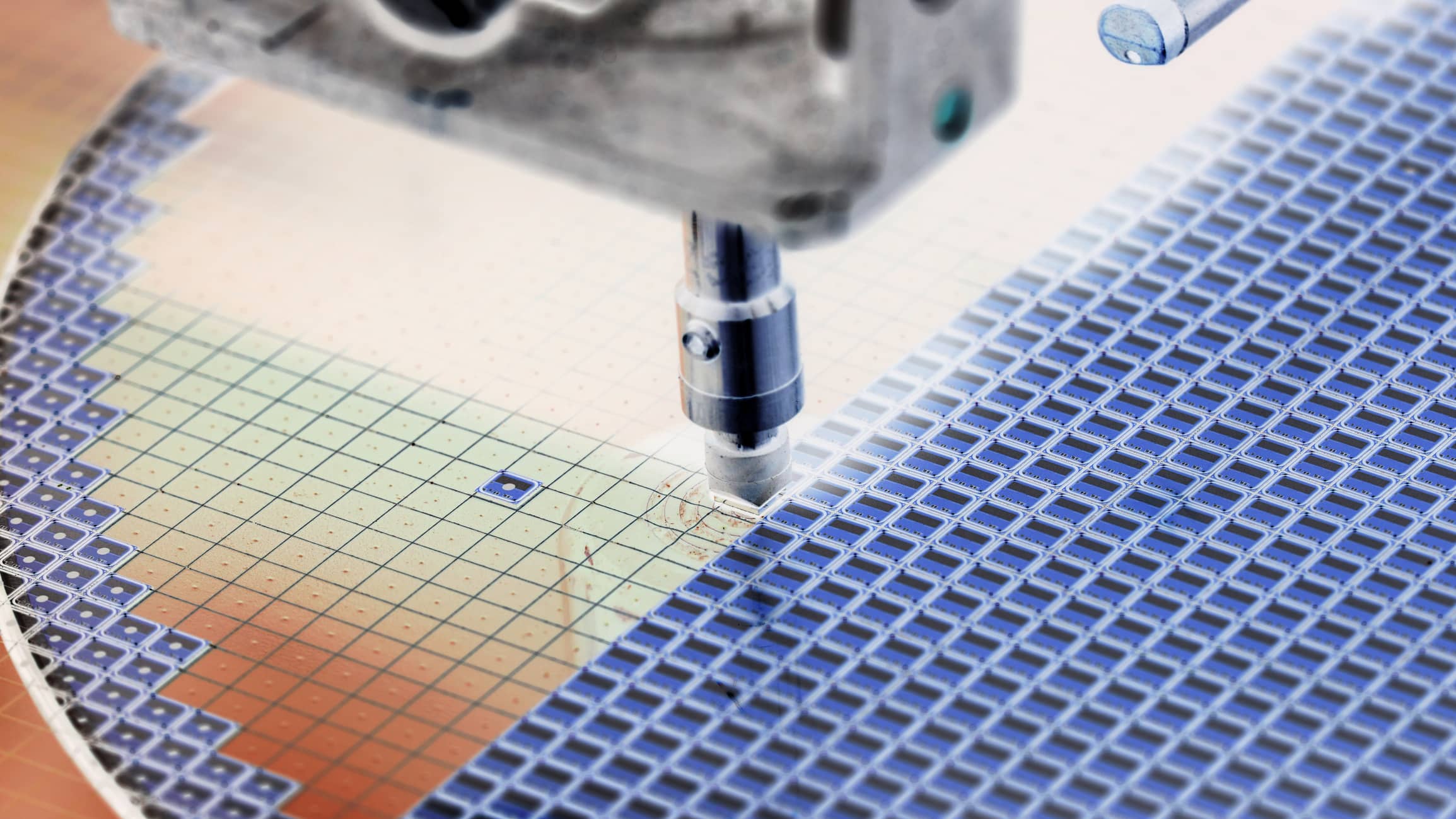
Wet Etching for MEMS Fabrication and Silicon Wafer Processing
Wet etching plays a critical role in MEMS fabrication and silicon wafer processing by enabling precise, selective material removal using controlled chemical reactions. Using chemistries such as KOH, TMAH, and buffered oxide etchants, our engineers create cavities, remove thin films, and define device structures with high selectivity and excellent surface quality.

Precision Wet Etch Services for MEMS Devices
Wet etching plays a critical role in MEMS fabrication and semiconductor wafer processing, enabling the formation of cavities, trenches, and structural features used in MEMS devices and sensor architectures. At Rogue Valley Microdevices, our MEMS foundry uses controlled chemical etching processes to selectively remove materials from silicon wafers and thin-film device layers.
Our wet etch capabilities support engineers developing MEMS sensors, microelectronic devices, photonic structures, and advanced semiconductor components. By combining proven wet bench processes with precise masking and process control, we deliver consistent wafer-level material removal while protecting critical device structures.
We perform all wet etch processing in our cleanroom MEMS fabrication environment, ensuring reliable results for both development programs and volume manufacturing.
Integrated MEMS Foundry Etch Capabilities
At Rogue Valley Microdevices, wet etching is part of our MEMS fabrication capabilities. Our engineers combine lithography, deposition, and Wet and dry etching processes to help customers move from early device development to production manufacturing.
Capabilities include:
- Silicon wet etching using KOH and TMAH
- Oxide etching using buffered oxide etchants (BOE)
- Metal etching for common thin-film materials
- Wafer-level process integration
- Development and production support
Our team works closely with customers to optimize etch chemistry, process conditions, and wafer handling to achieve reliable MEMS device performance
Metal Wet Etching
Wet chemical etching also enables selective removal of metal thin films used in microelectronic and MEMS structures.
Our process capability supports metal etchants for PVD deposited materials such as:
- Gold (Au)
- Chromium (Cr)
- Aluminum (Al)
Oxide Wet Etching
Buffered oxide etch (BOE) solutions selectively remove silicon dioxide layers from wafers. This process allows engineers to pattern oxide masks, open contact regions, or remove sacrificial oxide layers during MEMS fabrication.
Oxide wet etching supports several common fabrication steps, including:
- Opening contact windows
- Removing sacrificial oxide layers
- Patterning dielectric thin films
- Preparing surfaces for additional deposition processes
The ability to control oxide removal precisely allows engineers to integrate multiple dielectric layers within complex MEMS devices.
TMAH and KOH Silicon Etch for MEMS Fabrication
Silicon wet etching enables the formation of cavities, trenches, and structural features used in MEMS devices and sensor architectures. Our MEMS foundry supports both TMAH and KOH silicon etch on multiple wafer sizes.
These process techniques commonly supports fabrication steps such as:
- MEMS pressure sensor cavity formation
- Silicon membranes and diaphragms
- Microfluidic channels and reservoirs
- Structural features in MEMS accelerometers and inertial sensors
At Rogue Valley Microdevices, our MEMS foundry integrates TMAH and KOH silicon wet etch process techniques with photolithography, thermal oxidation, and LPCVD Nitride thin-film deposition to support advanced MEMS device fabrication on silicon wafers. These integrated wafer processing capabilities allow engineers to build complex microdevice architectures while maintaining precise control of etch depth, feature geometry, and wafer-level uniformity.
KOH Silicon Etching Services for MEMS Fabrication
Potassium hydroxide (KOH) creates anisotropic silicon etch profiles that follow the natural crystal orientation of silicon wafers. This wet etch process allows engineers to form well-defined cavities, V-grooves, and angled sidewalls with excellent dimensional control. Because KOH etches silicon at different rates along crystal planes, it enables precise shaping of microstructures used in MEMS sensors, microfluidic devices, and wafer-level microfabrication.
Engineers frequently select KOH silicon etching during MEMS fabrication when device designs require deep cavities, suspended membranes, or precisely defined structural features. The chemistry provides consistent etch rates and smooth silicon surfaces, which helps maintain tight tolerances across the wafer. By combining photolithography with robust masking layers, process engineers can selectively remove silicon while protecting critical device regions.
LPCVD silicon nitride often serves as a reliable etch mask during KOH silicon etching, allowing engineers to define complex device geometries with high precision. Patterned mask layers protect selected areas of the silicon wafer while exposed silicon etches along crystallographic planes to form predictable sidewall angles.
TMAH Silicon Etching for MEMS Fabrication
Tetramethylammonium hydroxide (TMAH) provides a highly controllable silicon wet etch process widely used in MEMS fabrication and silicon wafer processing. Engineers use TMAH to form well-defined cavities, trenches, and membranes in crystalline silicon wafers while maintaining smooth etched surfaces and predictable etch rates. Because TMAH produces anisotropic etch profiles that follow silicon crystal orientations, it enables precise formation of device features used in MEMS sensors, microfluidic devices, and microelectromechanical structures.
TMAH wet etching allows process engineers to shape silicon structures with excellent dimensional control during MEMS device fabrication. By combining patterned photoresist or oxide masks with controlled etch chemistry, engineers can selectively remove silicon while preserving critical device layers and surrounding structures.
Thermal silicon dioxide serves as an effective etch mask for TMAH silicon etching. Thick thermal oxide layers grown on silicon wafers provide strong resistance to TMAH chemistry, allowing engineers to protect selected wafer regions while exposed silicon areas etch anisotropically. When paired with photolithography, patterned thermal oxide masks enable precise definition of cavities, diaphragms, and suspended device structures.
These etch processes allow engineers to define conductive pathways, electrodes, bonding pads, and microelectronic structures on silicon wafers.