
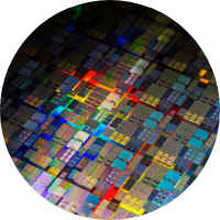
Comprehensive Silicon Wafer Processing Capabilities
We offer a range of wafer processing services designed to support MEMS development and semiconductor manufacturing workflows:
- Thermal oxide growth for dielectric layers and etch masking
- LPCVD polysilicon deposition for structural and conductive films
- LPCVD silicon nitride deposition for masking and stress-controlled layers
- PECVD thin films deposition as a standalone wafer processing step
- Metal deposition for electrical interconnects and device functionality
Each process operates with tight control over uniformity, repeatability, and material performance.
Flexible Wafer Processing for a Range of Device Applications
We support low, medium, and high volume wafer processing, enabling engineers to scale from development to production with confidence.
With deep process expertise and manufacturing knowledge, Rogue Valley Microdevices provides a reliable foundation for wafer-level process development and production.
Flexible Engagement Models
We support multiple project needs:
- Standalone wafer processing
- Process development and optimization
- Transition to integrated MEMS fabrication when required
Whether you require a single process step or plan to transition into full device fabrication, we provide flexibility without sacrificing quality.
Seamless Transition to MEMS Fabrication
Because wafer services operate within our MEMS foundry environment, we can seamlessly transition your project into full device fabrication.
Learn more about how thin films integrate into full MEMS fabrication: Thin Film Deposition
Wafer Services for MEMS and Sensor Manufacturing
Rogue Valley Microdevices provides precision wafer processing services for customers who require individual process steps without full device fabrication. Our wafer services deliver controlled, repeatable results using the same equipment and processes that support our MEMS foundry.
You can engage individual processes or integrate services into a larger fabrication flow depending on your project requirements.

Production-Grade Equipment and Process Control
Unlike standalone processing providers, we run wafer services on the same tools used for MEMS fabrication. This ensures consistency between development and production environments.
Our process control focuses on:
- Wafer-level uniformity
- Repeatable material properties
- Compatibility with downstream processing steps
This approach reduces variability and improves device performance.
Work With a Transparent Manufacturing Partner
We provide full visibility into how your wafers are processed. Our team communicates clearly, shares process insights, and collaborates to ensure your requirements are met.
We also support coordination with other foundries when needed to strengthen your supply chain resilience and ensure you meet market demands.
Thermal Oxidation
LPCVD Nitride Deposition
PECVD Film Deposition
Metal & Dielectric Film
