Photolithography
When it comes to MEMS, biomedical devices, and optical sensors, photolithography isn’t one-size-fits-all. Requirements may vary widely, depending on the design and function of your device. We have the capabilities to support you.
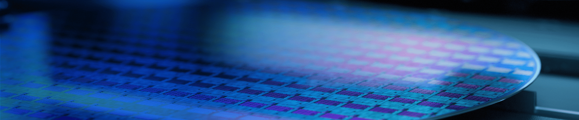
Photolithography for MEMS and Sensor Device Fabrication
Photolithography defines the patterns that form MEMS devices, sensors, and semiconductor structures. At Rogue Valley Microdevices, we perform precision photolithography on silicon wafers to support MEMS wafer fabrication and advanced microfabrication processes.
Our MEMS foundry uses photolithography to transfer mask patterns onto photoresist-coated wafers with high accuracy and repeatability. This core process capability allows engineers to define structural layers, electrical routing, cavities, and micro-scale device features, down to just a few microns
Because lithography controls device geometry and alignment accuracy, it plays a central role in MEMS manufacturing. Rogue Valley Microdevices integrates photolithography with thin-film deposition, plasma etching, metal lift-off and other wafer process steps to support both prototype development and production manufacturing.
We perform these wafer services in the same fabrication environment used for MEMS and sensor manufacturing, which ensures consistent process control and reliable device performance.
Contact and Proximity Photolithography for MEMS Devices
Many MEMS devices use micron-scale structures rather than nanometer-scale semiconductor nodes. Contact and proximity lithography provide a reliable and efficient solution for these applications.
Our contact aligners support:
- Front-to-Back Alignment Capability
- Feature sizes 5 µm and larger
- Excellent wafer-level uniformity
- Accurate mask alignment for multilayer devices
- Repeatable pattern transfer across silicon wafers
Engineers commonly use this lithography approach to fabricate pressure sensors, inertial sensors, microfluidic devices, and optical MEMS components.
Supported Wafer Sizes and Materials
- Silicon
- Silicon on Insulator
- Quartz
- Sapphire
- Glass
- GaN on Si
- Silicon Carbide
- Other specialty substrates
- Other specialty materials
- 100 mm wafers
- 150 mm wafers
- 200 mm wafers

MEMS Foundry Photolithography Services
Rogue Valley Microdevices provides flexible photolithography services for innovators, startups, universities, and established technology companies. Our engineers work directly with customers to optimize mask layouts, lithography parameters, and wafer process flows.
Because we operate a full MEMS fabrication environment, we integrate lithography with the complete process chain required to manufacture advanced MEMS devices.
This integrated approach helps customers move from device concept to volume manufacturing with greater speed and confidence.
Our photolithography tools support a wide range of MEMS fabrication processes and silicon wafer patterning requirements.
Capabilities include:
- Contact lithography for MEMS structures
- Proximity lithography for wafer patterning
- Multi-layer mask alignment
- Spin Coat Photoresist patterning for etch and lift-off processes
- Spray Coat Photoresist for high-topography structures
These capabilities allow engineers to build complex MEMS device architectures while maintaining precise alignment across multiple fabrication steps.