LPCVD Silicon Nitride Deposition for MEMS and Sensor Devices
Silicon nitride is a versatile thin film widely used in MEMS fabrication and sensor device manufacturing. LPCVD silicon nitride can serve as a structural layer for MEMS devices or as a passivation layer that protects sensitive device structures. Its tensile stress, mechanical strength, and excellent dielectric properties also make it valuable for balancing film stress within multilayer thin-film stacks.
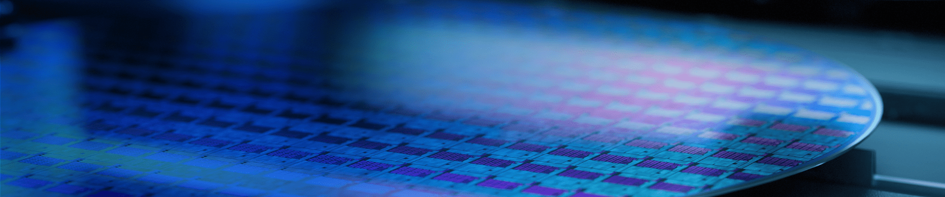
High-Quality LPCVD Silicon Nitride Deposition
At Rogue Valley Microdevices, we provide high-quality silicon nitride deposition on silicon wafers using advanced Low Pressure Chemical Vapor Deposition (LPCVD) processes. Our LPCVD silicon nitride films deliver the uniformity, mechanical stability, and electrical insulation required for advanced MEMS and sensors Devices.
Our LPCVD processes are optimized for consistent thin-film performance and excellent wafer-level uniformity, enabling engineers to integrate reliable silicon nitride layers into complex microdevice architectures.
With a wide range of silicon wafer sizes and nitride deposition options, we support both early-stage MEMS development and volume device manufacturing.
LPCVD Nitride Film Options
| Film Type | Films Stress | Max Thickness |
| Stoichiometric Nitride | => 800 MPa Tensile | 4,500Å |
| Low Stress Nitride | <250 MPa Tensile | 2µm |
| Super Low Stress Nitride | <100 MPa Tensile | 2µm |
Supported Wafer Sizes and Materials
- 50.8 mm wafers
- 76.2 mm wafers
- 100 mm wafers
- 125 mm wafers
- 150 mm wafers
- 200 mm wafers
- Silicon
- Silicon on Insulator
- Quartz
- Sapphire
- Other specialty materials
Electrical and Mechanical Properties
LPCVD silicon nitride is widely used in MEMS fabrication because it offers:
- Excellent film uniformity across the wafer
- Low pinhole density for reliable dielectric isolation
- High mechanical strength for MEMS structures
- Excellent chemical resistance for wet etch processing
- Stable electrical insulation properties
- Superior conformal coverage for complex structures
These properties make LPCVD silicon nitride wafers ideal for applications that require robust thin-film performance under demanding mechanical, electrical, and environmental conditions. For wafers that already have metal films, please see our list of PECVD film options.

Our engineers have decades of experience in developing and optimizing our LPCVD nitride films.
Silicon Nitride Wafer Applications
Silicon nitride thin films play a critical role in many microfabricated devices and semiconductor technologies. Our silicon nitride wafer deposition can be combined with other thin film deposition services like thermal oxidation to support applications including:
- MEMS pressure sensors
- Accelerometers and inertial sensors
- Microfluidic devices
- Optical MEMS components
- Low-loss optical waveguides for silicon photonics
- Devices passivation layers
- Dielectric isolation structures
- Membrane and diaphragm structures
Because LPCVD silicon nitride films provide high tensile strength and low permeability, they are widely used for MEMS membranes, structural layers, and protective coatings in advanced microdevices.
A MEMS Foundry Partner for Silicon Nitride Deposition
As a trusted MEMS foundry and wafer services partner, Rogue Valley Microdevices supports companies developing next-generation sensors, MEMS devices, and semiconductor technologies. Our LPCVD silicon nitride deposition services provide the film quality and process reliability needed to move efficiently from prototype development to scalable manufacturing.
Whether you need silicon nitride wafers for MEMS prototyping or a reliable deposition partner for other thin films like PVD metal and dielectrics, our team delivers the precision, consistency, and collaboration required for successful microfabrication.