Wafer Services for MEMS and Sensor Manufacturing
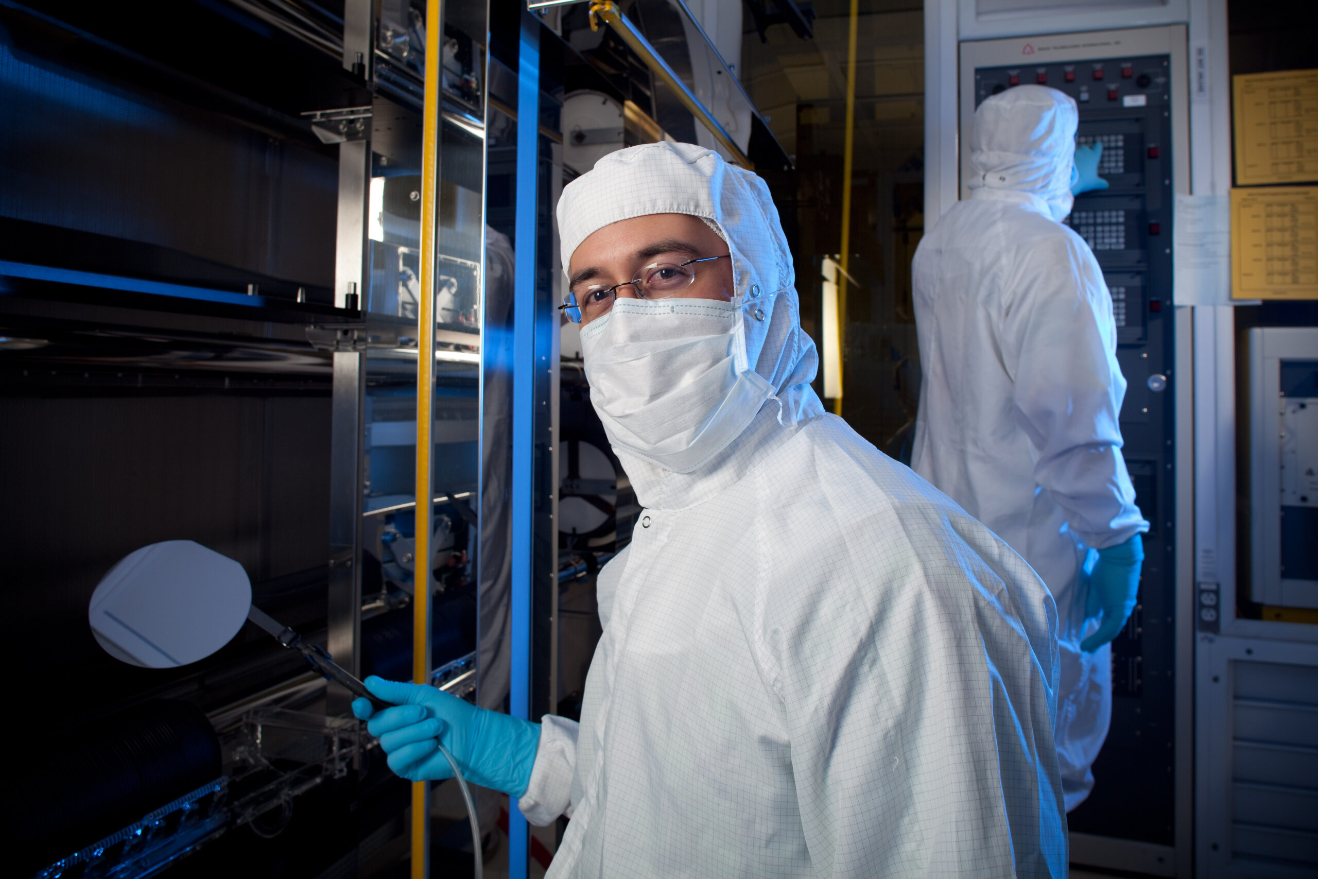
Rogue Valley Microdevices provides advanced wafer services for silicon wafer processing, MEMS fabrication, and semiconductor device manufacturing. Our foundry combines decades of process expertise with flexible manufacturing capabilities to help engineers transform ideas into reliable microfabricated devices.
We support a wide range of thin film deposition, thermal oxidation, and wafer-level processing services designed for MEMS sensors, microelectronic devices, and research applications. By integrating proven fabrication techniques with careful process control, we deliver consistent film quality, reliable wafer handling, and repeatable results across every project.
Whether you require a single wafer lot for early device development or consistent processing for production programs, our wafer services provide the precision and reliability required for advanced microtechnology.
Built for MEMS Device Development and Production
MEMS devices require precise control of materials, stress, film thickness, and wafer uniformity. Our fabrication environment supports these requirements through carefully maintained process equipment and proven wafer handling procedures.
Engineers rely on our wafer services to support:
- MEMS sensor fabrication
- Microelectromechanical actuator structures
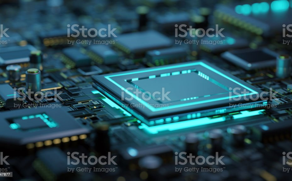
- Semiconductor device development
- Research and prototyping programs
- Pilot manufacturing and small-volume production
Our team collaborates closely with customers to align wafer processing with device architecture, materials selection, and downstream fabrication steps.
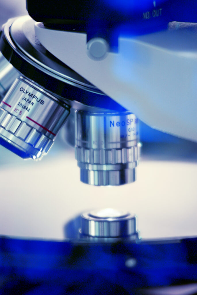
Comprehensive Silicon Wafer Processing Capabilities
Our wafer service platform connects engineers with a full range of front-end MEMS fabrication processes. Each service supports specific device structures, materials, and integration requirements used in modern microelectromechanical systems.
Our wafer processing capabilities include:
- Thermal Oxidation of Silicon Wafers
High-quality silicon dioxide growth for insulation layers, MEMS structures, and device passivation. - LPCVD Polysilicon Deposition
Uniform polysilicon films used for MEMS structural layers, sensors, and microactuators. - Silicon Nitride Deposition
LPCVD and PECVD nitride films for dielectric layers, diffusion barriers, and mechanical structures. - PECVD Thin Film Deposition
Low-temperature dielectric films including silicon oxide, silicon nitride, and silicon oxynitride. - Metal Deposition on Silicon Wafers
Conductive and barrier metal layers used for electrical interconnects and MEMS device integration.
Each wafer service supports multiple wafer diameters and flexible process parameters, allowing engineers to tailor film properties, thickness, and stress levels to match device performance requirements.
Flexible Wafer Processing for a Range of Device Applications
We support low, medium and high volume wafer processing, enabling engineers to scale from development to production with confidence.
Our wafer services support:
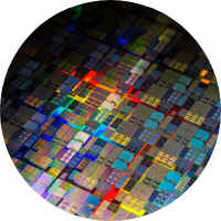
- Silicon wafers for MEMS fabrication
- Sensor device structures
- Semiconductor thin film processes
- Advanced microfabricated components
By combining thin film deposition expertise with MEMS fabrication knowledge, Rogue Valley Microdevices provides a reliable foundation for advanced device development and manufacturing.
Thermal Oxidation
LPCVD Nitride Deposition
PECVD Film Deposition
Metal & Dielectric Film